
Tech
The Complete Guide on Multi-layer PCB Board
Printed circuit boards are some of the essential components of modern electronics. However, there are different types of PCBs classified according to the design specifications, manufacturing processes, and application requirements.
One common type of printed circuit board used in various products is the multilayer printed circuit board. Here is a complete guide on the multilayer PCB board.
What is multilayer PCB?
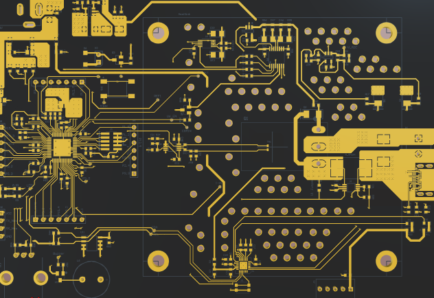
A printed circuit board is known as a multilayer if it has three or more sheets of copper foil insulated from each other and then joined together to form a piece. A multilayer PCB is more complex than single-layer PCBs and double-layer PCBs.
In a multilayer board, the outer layers are single-sided PCBs, while the inner layers are double-sided PCBs. Also, a few layers of multilayer PCBs allocated fixed tasks are known as planes. You can find ground planes or power planes.
Layers in multilayer boards are connected with each other in different styles that include buried via, blind via, or through hole via. A Via is a copper layered hole that connects several layers of multilayer PCB.
Typically, a multilayer PCB is rigid. This is because it is challenging to design a flexible multilayer PCB, especially when many layers exist. Keep in mind that some projects require more than 100 layers to be incorporated into one multilayer PCB.
But in most cases, four to eight layered printed circuit boards are used for common electronic gadgets. Nevertheless, you can find smart devices equipped with 12 layered PCBs.
Multilayer PCB manufacturing process
When it comes to the multilayer PCB manufacturing, several steps are involved. Below are the main steps of the multilayer PCB manufacturing process.
1. Finding a multilayer PCB manufacturer
When planning to produce multilayer PCBs, it is important to look for a reliable manufacturer. This is because various manufacturers offer different qualities and prices. Some things to check when looking for a PCB manufacturer include Via styles, Drill sizes, Maximum number of layers, and layer thickness.
2. Manufacturing of multilayer PCB
When it comes to the manufacturing of multilayer PCBs, special precaution is needed. This is because there are high chances of overlaps, cross connection, and tracing of copper, among other challenges.
In addition, the entire process should be done in a clean environment, and a special step up is required. Here are the steps involved in the manufacturing of multilayer PCB.
*Designing the software model – The first step of the multilayer PCB manufacturing process is to design the software model of the multilayer board. Various design tools are used to create a PCB layout. Some of them include Proteus, eagle, and Altium, among others.
Since multilayer PCB designs are a bit complex, experts and professional designers are needed. But once the designing process is complete, you can move to the next step.
*Making inner layer core – the next step is to make the inner layer core. The desired thickness is treated with copper foil, UV light, and dry film resist to make the inner core. The other is the machining process, including drill hole and CNC milling.
*Lamination – lamination involves prepreg sheets, inner layer core, and copper foil sheets. All these materials are fixed on each other where holes are used to align them.
For example, for a 4 layer board, a layer of copper foil is placed at the bottom, then prepreg sheets, then the inner layer core, more prepreg sheets are added, and finally, a copper foil sheet at the top.
*Applying pressure and heat – the next step is applying pressure, heat, and vacuum to get rid of trapped air between the layers. The process may take two hours or more, depending on the number of layers.
Resins join the sheets, foil, and sheets together to form a circuit board. Once the materials have cooled off, you will have a hard solid multilayer board.
*Testing – after manufacturing a multilayer PCB, the next step is to test whether the board is working as expected.
Benefits of multilayer PCBs
*Small size – the main advantage of a multilayer PCB is its small size. Since most modern electronic devices are being updated to be compact and slim, the small size of multilayer PCBs helps a lot.
*Light-weight – apart from being small, multilayer PCBs are lightweight. Thus, they can be used in hand-held gadgets such as blood pressure monitors, heartbeat monitors, smartphones, and electronic watches.
*High durability – since experts and professionals manufacture them, they are reliable and high quality. This means they can be used in complex devices and those used in harsh conditions.
*High-quality – due to the amount of work invested in designing and manufacturing multilayer PCBs, they tend to be of higher quality than single-sided PCBs and double-sided PCBs.
*More powerful – since there are many layers, multilayer PCBs can achieve greater capacity and speed even though they are lightweight and small.
Disadvantages of multilayer PCBs
*High manufacturing costs – the main advantage of multilayer PCBs is the cost. Since the manufacturing process is a bit complex, the cost is high.
*Increased manufacturing time – compared to single-layer PCBs and double-layer PCBs, multilayer printed circuit boards need more manufacturing time. This is because the process is a lengthy one. Moreover, it depends on the quality and the complexity of the board.
*Challenging to repair – since the manufacturing process is lengthy, it might be challenging to repair a multilayer PCB once it is manufactured. To overcome the challenge, manufacturing companies first design prototypes to remove the errors.
Applications of multilayer PCBs
Multilayer PCBs have become vital elements of modern electronic devices. From simple gadgets to complex electronic devices, you will find them in every sector. Here are some of the applications of multilayer PCBs.
*Consumer products – some of the consumer products designed using multilayer PCBs are computers, microwaves, mobile phones, home automation systems, and shaving machines, among others.
*Telecommunication systems – some telecommunication systems containing multilayer PCBs include radar systems, broadcasting systems, mobile transmission systems, and signal transmission systems.
*Medical devices – most smart medical devices have multilayer PCBs. Some medical devices to find multilayer circuit boards are blood pressure monitors, ECG, and heart rate monitors.
Final Word
Due to many new trends in the technology industry, multilayer PCBs provide a comprehensive solution. Although single-layer and double-layer PCBs have proven their ability, multilayer boards have numerous benefits.
Although they have some drawbacks such as increased costs, reliability and functionality are highly favored over cost. More people are willing to pay more for high-capacity electronic devices.
Kenneth is a proud native of sydney, born and raised there. However, he pursued his education abroad and studied in Australia. Kenneth has worked as a journalist for almost a decade, making valuable contributions to prominent publications such as Yahoo News and The Verge. Currently, he serves as a journalist for The Hear Up, where he focuses on covering climate and science news. You can reach Kenneth at [email protected].